Non-Ideal Operational Amplifiers
Table of Contents
1. Physical Op-Amp Model
A physical operational amplifier often consists of two or more blocks formed by:
- An operational transconductance amplifier (or OTA).
- A unity-gain buffer that copies the node voltage to the output without loading it.
The operational transconductance amplifier is essentially a voltage controlled current source: its output can be modeled as \(I=G_m(v_p-v_n)\). It has current output, so to convert this back to a voltage we can use a resistor \(R_x\) to ground. The capacitor \(C_x\) is added to provide a dominant pole so that high frequencies don’t cause the op-amp to become an oscillator. Since this is a current source, we usually choose the parallel resistance \(R_x\) to be very high in order to present a large output impedance.
Since we have a large output impedance, however, we need to also add a unity-gain buffer to prevent our circuits from loading the OTA. Many op-amps are internally constructed from an OTA and a buffer.
2. Op-Amp Non-Idealities
When we analyzed a ideal op-amp, we made a few assumptions on properties that differ in the real world:
| Property | Ideal | Real |
|---|---|---|
| Gain | \(\infty\) | Finite |
| Bandwidth | \(\infty\) | Finite |
| \(Z_{in}, Z_{out}\) | \(\infty, 0\) | Finite |
| Offset voltage | 0 | mV-level |
| Input bias current | 0 | pA to uA |
| Output swing | unlimited | limited by supply |
| Slew rate | unlimited | limited |
In particular, we have already seen how we can use negative feedback to decouple the closed-loop gain from the non-ideal open-loop gain of the op-amp, provided that the open-loop gain is very large.
2.1. Gain-Bandwidth
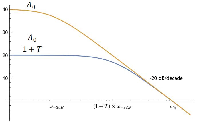
Using our OTA plus unity buffer model, by Ohm’s Law we can derive the gain to be \(A_0 = G_mR_x\). The capacitor provides us with a pole whose cutoff frequency is \(\omega_c = \frac{1}{R_xC_x}\). An interesting observation is that the gain-bandwidth product depends only on the values of \(G_m\) and \(C_x\):
\begin{align} A_0\omega_c = \frac{G_m}{C_x} \end{align}We can increase our bandwidth by around \(1 + \beta A_0\) if we use negative feedback, but our gain drops by the same factor making the GBW product constant:
2.2. Offset Voltage
Real op-amps often have a nonzero DC offset voltage. This offset voltage can often be trimmed by connecting a potentiometer to the two offset-nulling terminals of the op-amp. The wiper of the potentiometer is connected to the negative supply of the op-amp.
2.3. Slewing
Real amplifier output is limited by its slew rate, or the maximum rate of change at the output:
\begin{align} \text{SR} = \frac{\text{d}V_o}{\text{d}t} \end{align}This is often specified in datasheets in units of \(\frac{\text{V}}{\mu \text{s}}\). Since the OTA can only supply a limited amount of current, slewing comes from the fact that the change in the voltage of the capacitor in the OTA is limited based on \(I_{\text{max}}=C_x\frac{\text{d}V}{\text{d}t}\).